


Nisshinbo RP120Z LDO Regulators
Nisshinbo RP120Z LDO (Low-Dropout) Regulators are designed to operate at an input voltage as low as 0.768V. The RP120Z LDO Regulators use an internal low on-resistance NMOS transistor as a driver. The VBIAS pin provides the higher supply necessary for the LDO circuitry while the output current comes directly from the VIN input for high-efficiency regulation. These devices feature a high Power Supply Rejection Ratio (PSRR), high output current, and fast response characteristics.
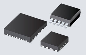
The Nisshinbo RP120Z LDO Regulators are offered in a compact 1.2mm x 0.8mm Wafer Level Chip Scale Package (WLCSP), ideal for space-constrained applications.
Features
- Input voltage range
- VIN = VSET + VDIFF to VBIAS
- (Ex. Min. 0.768V @ VSET = 0.6V, VBIAS = 3.3V, IOUT = 1.5A)
- VBIAS = 2.4V to 5.5V
- 0.6V to 3.6V external setting range of output voltage
- Output current: IOUTMAX = 1.5A
- 35µA supply current
- 50µVrms (VSET = 0.6V) output noise
- 67mV dropout voltage (IOUT = 1A, VSET = 0.6V, VBIAS = 3.3V)
- Power supply ripple rejection
- 90dB (f = 1kHz, ripple in VIN)
- 60dB (f = 100kHz, ripple in VIN)
- 600mA inrush current limit
- 600mA short circuit current protection
- 165°C thermal shutdown
- COUT 7µF ceramic capacitor
- -40°C to +125°C junction temperature range
- 1.2mm x 0.8mm x 0.29mm WLCSP-6-P11 package
Applications
- Portable communication devices, battery-powered devices, cameras, media players
- Communication devices such as RF modules
- Clock generation devices such as VCOs and PLLs
- Constant voltage source for analog circuits of FPGAs and SoCs
Typical Application Circuit

Block Diagram

Package Outline

Publicado: 2021-12-16
| Actualizado: 2022-03-11