


onsemi NL3V8T24x 8-Bit Dual-Supply Level Translators
onsemi NL3V8T24x 8-Bit Dual-Supply Level Translators are 8-bit configurable, high-performance devices with 3-state outputs designed to facilitate seamless voltage level translation between two logic domains in digital systems. The A- and B-ports are designed to track two different power supply rails, VCCA and VCCB, respectively. Configurable from 0.9V to 3.6V, both supply rails allow universal voltage level translation between the A- to B-ports. The NL3V8T244 allows non-inverting translations from the A- to B-ports, while the NL3V8T240 allows inverting translations. With fast propagation delays and low power consumption, these onsemi level translators are well-suited for applications in mobile devices, consumer electronics, and embedded systems requiring reliable and flexible voltage interfacing.
Features
- Wide 0.9V to 3.6V VCCA and VCCB operating range
- ±24mA balanced output drive at 3.0V
- High-speed with balanced propagation delay, 2.8ns maximum at 3.0V to 3.6V
- Inputs pins Overvoltage Tolerant (OVT) to 3.6V
- Non-preferential VCC sequencing
- Outputs at 3-state until an active VCC is reached
- Partial power-off protection
- Outputs switch to 3-state with either VCC at GND
- Typical maximum data rates
- 380Mbps (≥1.8V to 3.3V translation)
- 200Mbps [≥1.1V to (1.8V, 2.5V, 3.3V) translation]
- 150Mbps (≥1.1V to 1.5V translation)
- 100Mbps (≥1.1V to 1.2V translation)
- UL 94V-0 flammability rating
- Moisture Sensitivity Level (MSL) 1
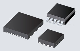
- Small UDFN20, SOIC-20W, or TSSOP-20 package options
- Lead-free, Halogen-free/BFR-free, and RoHS-compliant
Applications
- Mobile phones, PDAs, and other portable devices
- Automotive
- Industrial
Specifications
- ±100mA maximum latchup performance
- 0nS/V to 5nS/V input transition rise/rate
- Input leakage current
- ±1.0µA from -40°C to +85°C
- ±5.0µA from -40°C to +125°C
- 2.5pF control pin input capacitance
- 5.0pF I/O pin input capacitance
- 12pF power dissipation capacitance
- Maximum ESD
- 2kV Human Body Model (HBM)
- 1kV Charged-Device Model (CDM)
- -40°C to +125°C operating temperature range
Logic Diagrams

Pin Assignments

Publicado: 2025-08-07
| Actualizado: 2025-09-10