
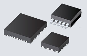


onsemi NVBYST0D6N08X 80V N-Channel Power MOSFET

onsemi NVBYST0D6N08X 80V N-Channel Power MOSFET offers a low QRR and soft recovery body diode in a TCPAK1012 (TopCool) package. This MOSFET has a low RDS(on) to minimize conduction losses and a low QG and capacitance to minimize driver losses. The onsemi NVBYST0D6N08X is AEC-Q101 qualified, PPAP capable, lead-free, Halogen-free/BFR-free, and RoHS-compliant. A typical application for this MOSFET is Synchronous Rectification (SR) in DC-DC and AC-DC, a primary switch in an isolated DC-DC converter, motor drives, and automotive 48V systems.
Features
- Low QRR, soft recovery body diode
- Low RDS(on) to minimize conduction losses
- Low QG and capacitance to minimize driver losses
- AEC-Q101 qualified and PPAP capable
- Lead-free, halogen-free/BFR-free, and RoHS-compliant
Applications
- Synchronous Rectification (SR) in DC-DC and AC-DC
- Primary switch in an isolated DC-DC converter
- Motor drives
- Automotive 48V system
Specifications
- 80V (max.) drain-to-source voltage (VDSS)
- 20V (max.) gate-to-source voltage (VGS)
- 767A (max.) continuous drain current (ID) at TC = +25°C, 542A at TC = +100°C
- 750W (max.) power dissipation (PD) at +25°C
- 2443A (max.) pulsed drain current (IDM) at TC = 25°C, tp = 100µs
- -55°C to +175°C operating junction (Tj) and storage temperature range (Tstg)
- 0.56mΩ (typ.) drain-to-source on resistance [RDS(on)] (VGS = 10V, ID = 80A, TJ = +25°C)
- 16419pF (typ.) input capacitance (CISS) (VDS = 40V, VGS = 0V, f = 1MHz)
- 4654pF (typ.) output capacitance (COSS) (VDS = 40V, VGS = 0V, f = 1MHz)
- 228nC (typ.) total gate charge [QG(TOT)] (VDD = 40V, ID = 80A, VGS = 10V)
Circuit/Marking Diagrams

Publicado: 2025-11-24
| Actualizado: 2025-12-26