
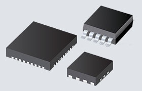


Texas Instruments TLVM1440x Dual/Single Output Power Modules
Texas Instruments TLVM1440x Dual/Single Output Power Modules are highly integrated, 36V input capable, DC-DC design that combines power MOSFETs, a shielded inductor, and passives in an enhanced HotRod™ QFN package. The device supports either dual output or a high current single output using an interleaved, stackable, current-mode control architecture for easy loop compensation, fast transient response, excellent load, and line regulation. The module has VIN and VOUT pins at the package's corners for optimized input and output capacitor placement. A large thermal pad beneath the module enables a simple layout and easy manufacturing handling.
With an output voltage from 1V to 9V, the Texas Instruments TLVM1440x is designed to quickly and easily implement a low-EMI design in a small PCB footprint. The total design requires as few as six external components and eliminates the magnetics selection from the design process.
Even though these are designed for small size and simplicity in space-constrained applications, the TLVM1440x modules offer many features for robust performance: precision enable with hysteresis for adjustable input-voltage UVLO, along with integrated VCC, bootstrap, and input capacitors for increased reliability and higher density. These modules are configured to automatically switch between constant switching frequency (FPWM) at higher loads and variable frequency (PFM) for higher light load efficiency. These also include a PGOOD indicator for sequencing, fault protection, and output voltage monitoring.
Features
- Versatile dual output voltage or single output synchronous buck module
- Integrated MOSFETs, inductor, and controller
- Wide input voltage range of 3V to 36V
- Adjustable output voltage from 0.8V to 9V
- 6.5mm × 7.0mm × 2mm overmolded package
- –40°C to 125°C junction temperature range
- Ultra-high efficiency across the full load range
- Peak efficiency of 93.5%
- External bias option for improved efficiency
- Exposed pad for low thermal impedance. EVM θJA = 20°C/W.
- Shutdown quiescent current of 0.6µA (typical)
- Ultra-low conducted and radiated EMI
- Low-noise package with dual input paths and integrated capacitors reduces switch ringing
- Meets CISPR 11 and 32 Class B emissions
- Inherent protection features for robust design
- Precision enable input and open-drain PGOOD indicator for sequencing, control, and VIN UVLO
- Overcurrent and thermal shutdown protections
Applications
- Test and measurement, aerospace and defense
- Factory automation and control
- Buck power supplies
Functional Block Diagram
